



 This image is released under a
 Digital image sensor
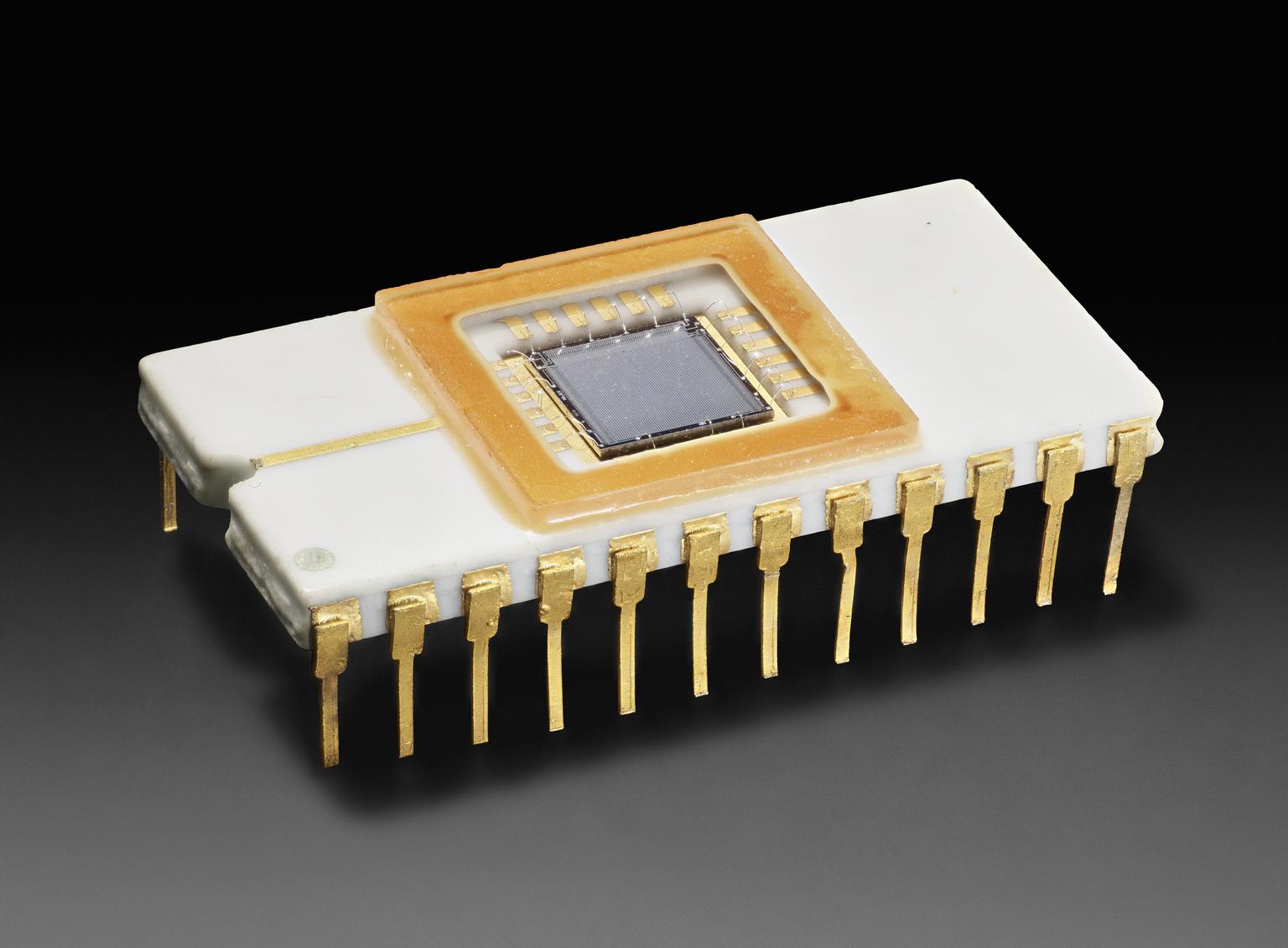
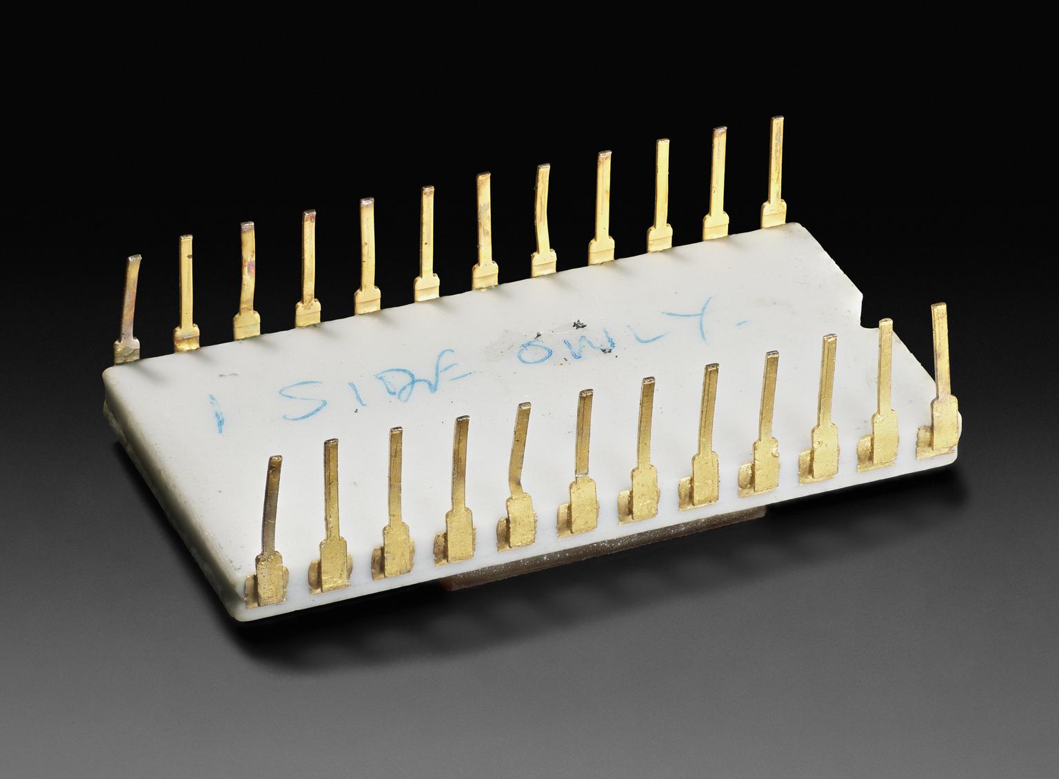
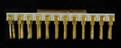
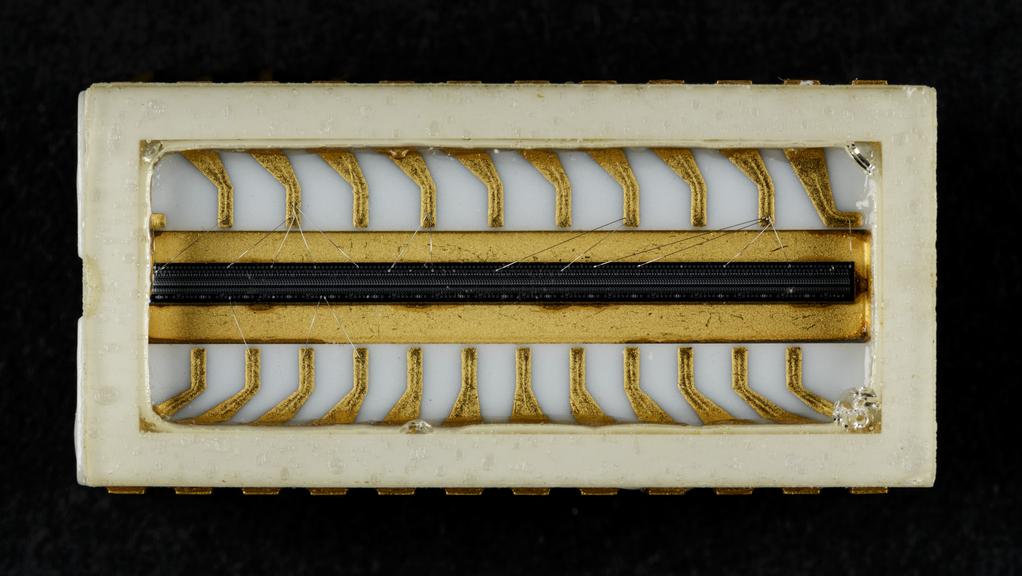
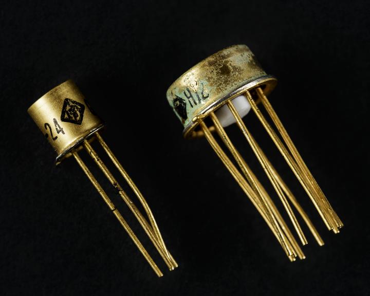
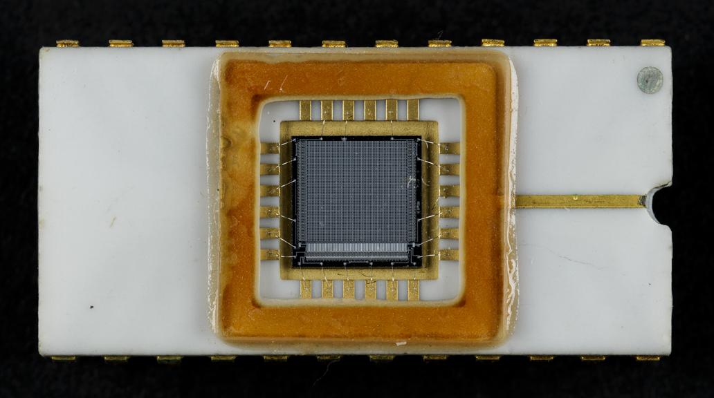
Optical digital sensor, light switch, manufactured in the UK by Integrated Photomatrix Ltd, 1969, from the collection of Peter Noble.
More
While looking for a way to convert words written on paper into electronic numbers a computer could understand, engineer Peter Noble became one of a handful of people around the world who were taking the first steps in digital photography. Seeing a gap in the market, he started a new company in 1968 to develop and sell image sensors that could convert energy from light into electrical energy. His business, integrated Photomatrix Ltd was successful, but making sensors that were good enough quality for cameras proved difficult. Manufacturing techniques needed to develop before the sensors could be mass-produced cheaply enough to be profitable.
In the early sensors the tiny amount of light hitting each pixel was too weak to make a strong electrical signal. Peter Noble’s team's breakthrough was to invent the active pixel. Each pixel on the sensor was loaded up with electricity so that when light struck it, it allowed the electricity already there to flow. In the UK, Peter Noble struggled to fund further development of the active pixel. Meanwhile in the USA an alternative system using of ‘charge-coupled devices’ (CCDs) in sensors was emerging. Though subtly different, both systems use microchips divided into grids of pixels, and both are now used in billions of digital cameras around the world.